Modelling Approach
PCB-modelling
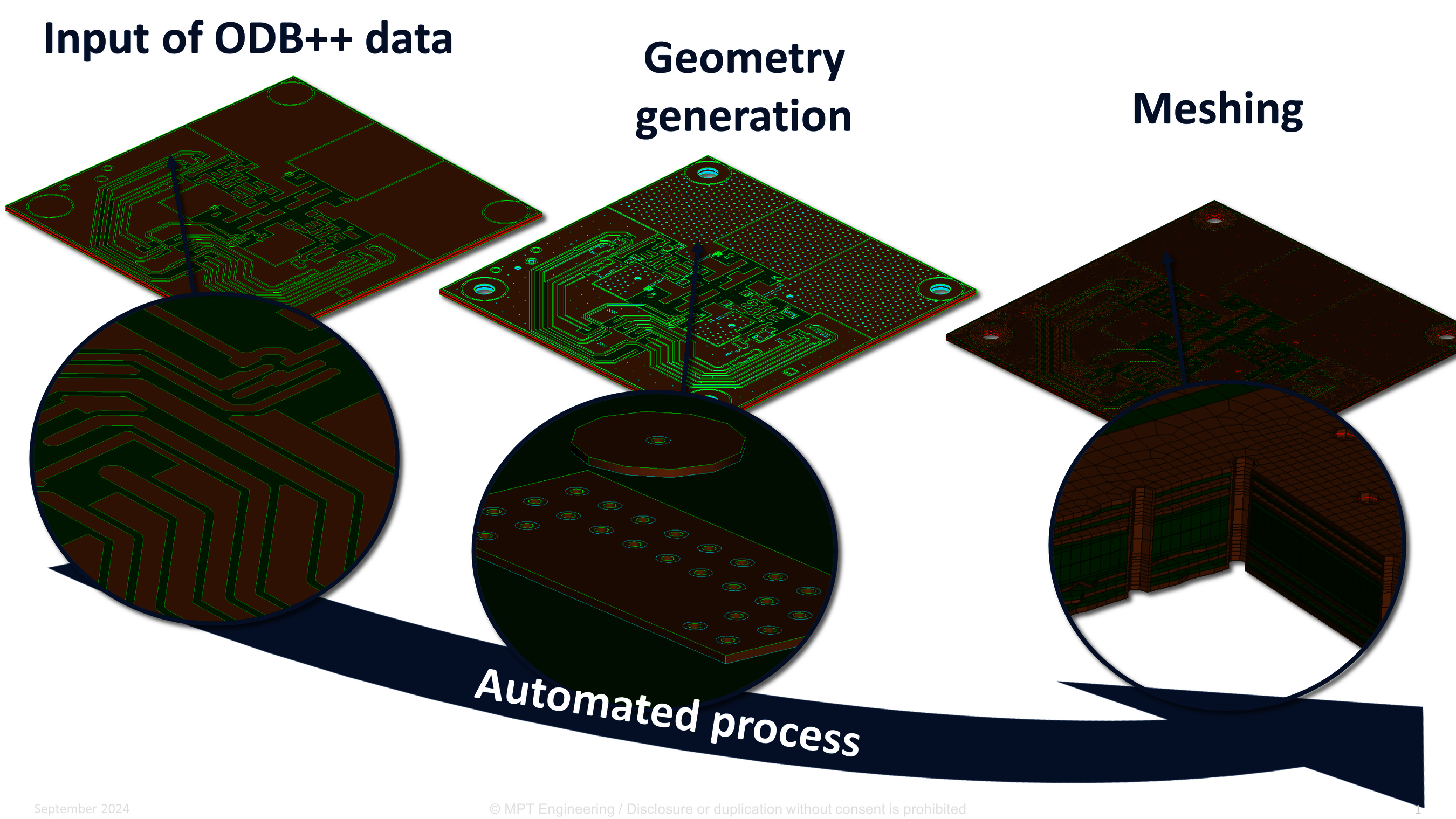
Shows the modelling process for creating a detailed FE mesh of a circuit board. The first two images still show the geometry of the board, the third image shows an FE mesh of the board.
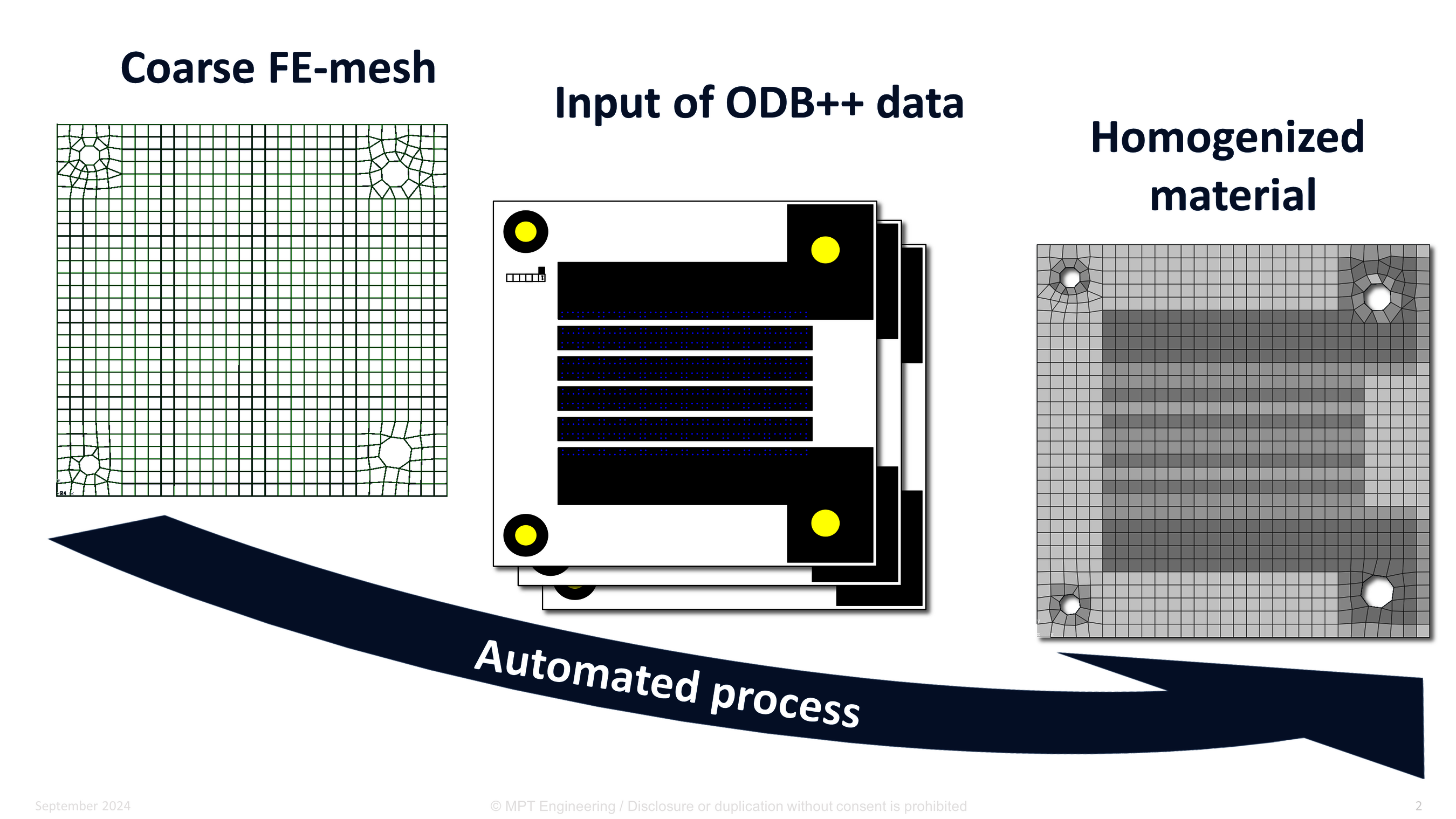
Shows the modelling process for creating a simple FE mesh of a board containing the inhomogeneous material distribution from the board data (ODB++). The shades of grey in the third figure represent the respective stiffness values.
Fine modelling
After reading the ODB++ data the automated process begins generating a 2D geometry of the profile for each layer of the PCB. In a further step all features of the PCB (traces, vias, holes, etc…) are projected onto the corresponding layers. An algorithm determines the necessary mesh size for different features of the PCB, making it finer in complex regions and coarser in simpler ones. The resulting 2D geometry of each layer is then meshed and extruded. Finally, the correct materials get assigned to the corresponding parts of the mesh.
The resulting finite element model contains all details of the PCB and is therefore typically large. When modelling bigger PCBs it is necessary to reduce the model size. This can be achieved by using a material homogenization process.
Homogenization
For most simulation use-cases it is necessary to reduce the model size while still maintaining the complex PCB characteristics. This is achieved by the material homogenization approach which uses the boundaries of every finite element from the PCB model to identify enclosed sections from the ODB++ data. Based on this enclosed geometry and material information one effective orthotropic material will be calculated for every element considering parallel and serial material combination in every dimension. This is achieved by using modified Reuss (isostress) or Voigt (isostrain) formulars.
SMD-modelling
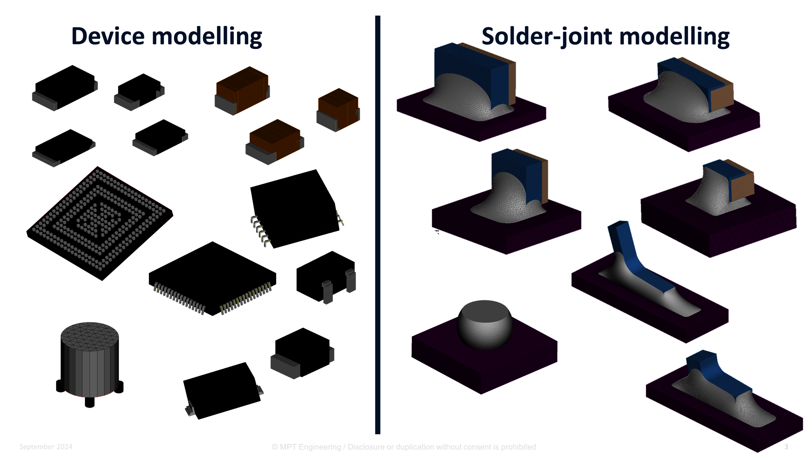
Left: Shows different SMD types modelled from beam and shell elements
Right: Shows the corresponding fine FE models of the solder joints
Shows an animation of the generation of a solder joint structure with the SurfaceEvolver software
A database is used to store finite element models of SMDs. For each SMD package type this database contains a simplified model of the device itself and a detailed solder joint model.
Device modelling
If a new SMD package needs to be added to the database, its geometry data has to be specified according to the datasheet. An algorithm uses this data as an input and automatically generates a simplified SMD model with beam and shell elements and adds it to the database for further use.
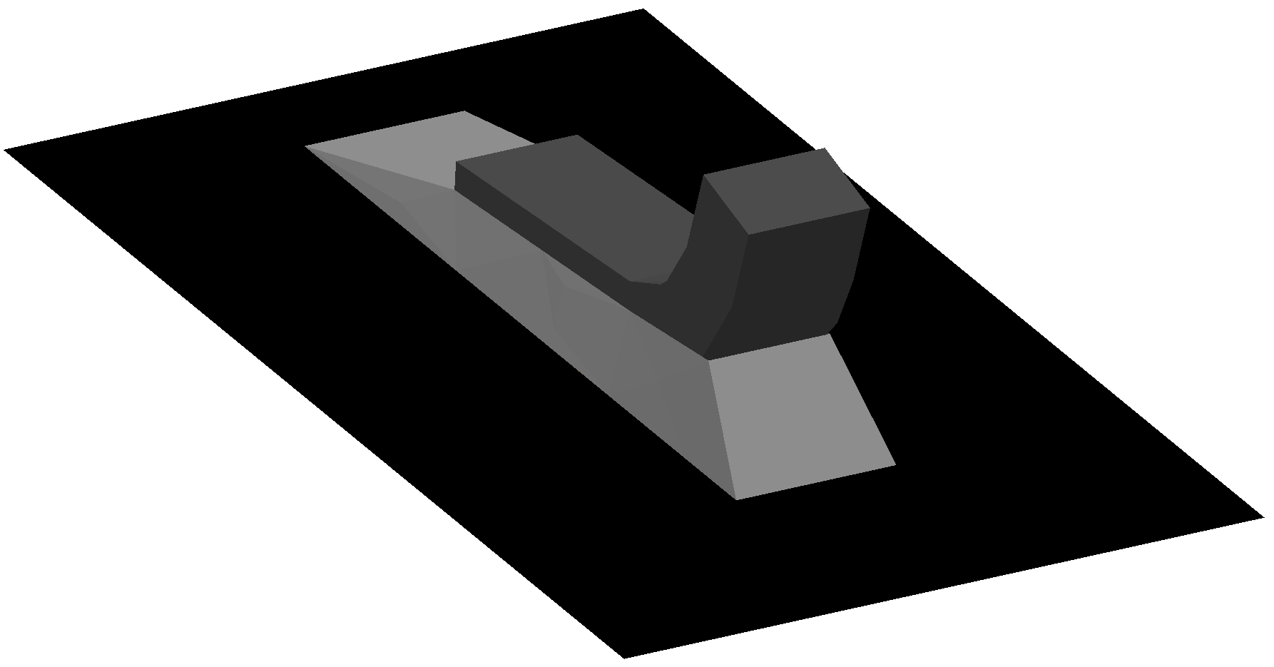
Solder-joint modelling
The shape of the solder joint depends on the solder-type and the size of the solder pad. After specifying this data, the automated process utilizes a parametric CAD model as well as a parametric solder joint FE-model of the corresponding solder-type. The solder meniscus shape is automatically calculated taking physical parameters like surface tension during the soldering process and gravity into consideration. The resulting geometry of the solder meniscus is imported into the FE-preprocessor where it is automatically meshed and stored in a database similar to the simplified SMD model.
Interested in more?
Applications
Modules